
��ϵ��ʽ
more��������Ӣ������
- 2017-09-10��������������Ϣϵͳ��Ŀ��..
- 2016-07-10���������רҵԤ�ƿγ���ҵ..
- 2016-04-21����http iap�������ʵ��
- 2016-04-14�������пͻ���ȫ����ʶ����
- 2015-11-16computer science essay-��..
- 2015-10-19Ӣ��������அ�IՓ�Č���ע..
- 2015-05-30network development manag..
- 2015-03-01������Ӿ���ͼ����Ӱ������..
- 2014-08-14Ӣ����ѧ����-���������Ӱ..
- 2014-08-06Ӣ����ѧ�������רҵ����
more��������
- 2010-12-23���ڼ�������������Ŀ�����..
- 2014-07-31�����������ѧ������-�Ƽ�..
- 2014-08-14Ӣ����ѧ����-���������Ӱ..
- 2015-05-30network development manag..
- 2010-12-23���ü�����������������..
- 2014-08-06Ӣ����ѧ�������רҵ����
- 2014-04-21������������computer ne..
- 2011-02-22audio fingerprinting:near..
- 2011-01-23��ѧ����������һ����άģ��..
- 2011-04-19please find below eamples..
more��ѧ����д��ָ��
- 2024-03-31��ɭ•����˹С˵��..
- 2024-03-28��������Ů����������˼����..
- 2024-03-27����·�����ء�֯�����ϡ���..
- 2024-03-21��Խ���ӣ��ۡ����������ˡ�..
- 2024-03-19�����˱���•�Ѷ�����..
- 2024-03-13�������֮�á����ӿ�������..
- 2024-02-22��ѧ����ѧ�ӽ��µġ�ӡ��֮..
- 2023-05-03Ӣ�������ʶ���֮���ݴ�����..
- 2023-02-07Ŀ����������5g��the futur..
- 2022-07-04����Ӣ�����������ѧϰ�ߵ�..
����HTTP IAP�������ʵ�� [4]
�������ߣ�Qingqing Xu�������ԣ�ְ������ Scholarship Papers�dz�ʱ�䣺2016-04-21�༭��anne����ʣ�10200
����������2850���ı�ţ�org201604201253338185���֣�Ӣ�� English������Ӣ���۸��������
ժҪ��IAP����Ӧ�ó�����Ƕ��ʽ��Ʒ�Ĺ̼����³���ķ�����ͨ������Զ�̸���Ƕ��ʽ��Ʒ�Ĺ̼������ڱ��Խ��Խ�����ˡ�
by MEMP_NUM_TCP_PCB
c) the heap size, defined by MEM_SIZE
d) the number of buffers, defined by PBUF_POOL_SIZE, and the buffer size, defined by PBUF_POOL_BUFSIZE
The number of buffers and the heap size allocated to the application depend on the application��s performance, simultaneous connection requirements and available RAM. Increasing these parameters (number of buffers and heap size) boosts the application performance and connectivity, but reduces the amount of available RAM. Conversely, decreasing these parameters increases the available RAM space, but limits the application performance and connectivity[5].
4) STM32F107 hardware checksum
Porting LwIP to the STM32F107 takes advantage of the advanced features of the STM32F107's Ethernet controller��s capability of generating, inserting and verifying the checksums of the IP, and TCP protocols by hardware. This feature frees some CPU load and improves the performance of the IAP program[6].
We can enable the checksum by hardware by uncommenting #define CHECKSUM_BY_HARDWARE in the lwipopts.h file.
The STM32F107��s checksum by hardware feature can be enabled by setting:
a) the CIC bits, in the first word of the Tx descriptor, for transmitted frames.
b) the IPCO bit, in the ETH_MACCR register, for received frames.
For those MCU without hardware checksum capability, software generation and checksum verification for the IP, UDP and TCP protocols can be enabled by commenting #define CHECKSUM_BY_HARDWARE in the lwipopts.h file. But it will add some CPU load and decrease the performance of the IAP program.
B. IAP program implementation
This IAP implementation allows the user to select a binary file with a web browser and to upload it to the embedded system. The IAP firmware can receive a binary file with HTTP protocol and program it into STM32 Flash memory automatically.
1) Firmware code layout in flash
Because the interrupt vector table of STM32F107 is at the lowest address of the program memory space[6], in order to make the IAP code response to interrupt correctly, the IAP code is placed at the base address of the flash memory. With the size not exceeding the total size of user flash area, the compiled user application code is placed right after the IAP code (figure 4).
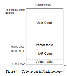
Figure 4. Code layout in Flash memory
The first part of code must be downloaded to MCU with other ways, like JTAG or ISP. The second part of code can use the IAP function of the first part of code. Or it can be downloaded to MCU together with the first part of code, and be updated later with the IAP function of the first part of code.
Before the second part of code starts to run, it should remap the interrupt vector table of CPU to its own interrupt vector table. Then it can do other following operations.
The user application software is compiled and linked to run from the base address of the user Flash area. So, the jump address of IAP code must be equal to the user application link starting address, or the application program cannot be started up correctly[8]. In this IAP implementation, both of the IAP jump address and the base address of the user application program interrupt vector table are 0x8002000, because the user application program start address in the flash is equal to 0x8002000.
2) File upload using HTTP
File up��������Ӣ���������ṩ�������ṩ���Ĵ�д��Ӣ�����Ĵ�д����д��������дӢ����������д��ѧ����������дӢ����������ѧ�����Ĵ�д��غ��Ĺؼ���������
c) the heap size, defined by MEM_SIZE
d) the number of buffers, defined by PBUF_POOL_SIZE, and the buffer size, defined by PBUF_POOL_BUFSIZE
The number of buffers and the heap size allocated to the application depend on the application��s performance, simultaneous connection requirements and available RAM. Increasing these parameters (number of buffers and heap size) boosts the application performance and connectivity, but reduces the amount of available RAM. Conversely, decreasing these parameters increases the available RAM space, but limits the application performance and connectivity[5].
4) STM32F107 hardware checksum
Porting LwIP to the STM32F107 takes advantage of the advanced features of the STM32F107's Ethernet controller��s capability of generating, inserting and verifying the checksums of the IP, and TCP protocols by hardware. This feature frees some CPU load and improves the performance of the IAP program[6].
We can enable the checksum by hardware by uncommenting #define CHECKSUM_BY_HARDWARE in the lwipopts.h file.
The STM32F107��s checksum by hardware feature can be enabled by setting:
a) the CIC bits, in the first word of the Tx descriptor, for transmitted frames.
b) the IPCO bit, in the ETH_MACCR register, for received frames.
For those MCU without hardware checksum capability, software generation and checksum verification for the IP, UDP and TCP protocols can be enabled by commenting #define CHECKSUM_BY_HARDWARE in the lwipopts.h file. But it will add some CPU load and decrease the performance of the IAP program.
B. IAP program implementation
This IAP implementation allows the user to select a binary file with a web browser and to upload it to the embedded system. The IAP firmware can receive a binary file with HTTP protocol and program it into STM32 Flash memory automatically.
1) Firmware code layout in flash
Because the interrupt vector table of STM32F107 is at the lowest address of the program memory space[6], in order to make the IAP code response to interrupt correctly, the IAP code is placed at the base address of the flash memory. With the size not exceeding the total size of user flash area, the compiled user application code is placed right after the IAP code (figure 4).
Figure 4. Code layout in Flash memory
The first part of code must be downloaded to MCU with other ways, like JTAG or ISP. The second part of code can use the IAP function of the first part of code. Or it can be downloaded to MCU together with the first part of code, and be updated later with the IAP function of the first part of code.
Before the second part of code starts to run, it should remap the interrupt vector table of CPU to its own interrupt vector table. Then it can do other following operations.
The user application software is compiled and linked to run from the base address of the user Flash area. So, the jump address of IAP code must be equal to the user application link starting address, or the application program cannot be started up correctly[8]. In this IAP implementation, both of the IAP jump address and the base address of the user application program interrupt vector table are 0x8002000, because the user application program start address in the flash is equal to 0x8002000.
2) File upload using HTTP
File up��������Ӣ���������ṩ�������ṩ���Ĵ�д��Ӣ�����Ĵ�д����д��������дӢ����������д��ѧ����������дӢ����������ѧ�����Ĵ�д��غ��Ĺؼ���������
 Ӣ��
Ӣ�� �Ĵ�����
 ����
���� ���ô�
���ô� ������
 �¼���
�¼��� ���
��� �ձ�
�ձ� ����
���� ����
���� �¹�
�¹� ������
 ��ʿ
��ʿ ����
���� ����˹
����˹ ������
 ��������
 �Ϸ�
�Ϸ�